What’s All This FECi Stuff
1.6Tb class modules are now being developed to meet the raw bandwidth and bandwidth density demands of applications including ‘factory scale’ AI and hyperscale computing. Based on emerging standards from IEEE and OIF, they build upon a solid 800Gb ecosystem and include several new features – both evolutionary and revolutionary.
224G Signaling and FECi
The most obvious change is the move to 224G signaling. At 1.6Tb, we will see two new speeds: eight lanes of 212.5Gb/s for the host-to-module interface and 226.875Gb/s for some optical interfaces. The faster 226.875Gb rate introduces a revolutionary aspect for client optics: an inner FEC, known as FECi.
The host interface based on 212.5Gb already uses the well-established RS FEC for error protection. This FECo, an outer FEC, is used on all interfaces, while certain optical PMDs require higher coding gain provided by the additional FECi. What adds to the revolutionary aspect of the FECi is the use of a soft-decision Hamming (128,120) code. The use of the soft-decision FEC means close coupling of the PAM-4 RX PHY and the FECi decode logic to achieve maximum coding gain. While this soft-decision approach may have a small power burden, the coding gain impact for interfaces is meaningful.
This FECi functionality is implemented inside the optical module because it is PMD dependent, which drives new complexity for module development, testing and validation. In addition to the development and testing of the new complex FECi functional logic, there is additional module F/W needed to support this, especially for reporting FEC RX parameters.
Symbol Mux Over Classic Bit Mux
Another change is the move to symbol mux over the classic bit mux used at 800Gb and below. This approach will help extract additional benefits in error reduction.
VIAVI has been the reference for both client and digital coherent module development, testing and validation since the early days of 100G. We have always taken an integrated approach, including PHY, photonics and firmware.
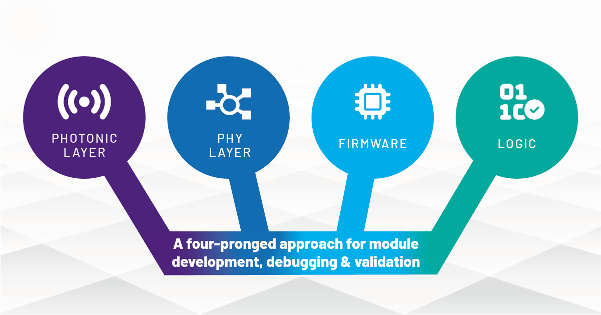
This integrated approach is more critical than ever. Our experience with FEC logic stress and validation will now play a role as FECi logic and performance must be validated at the module level. Therefore, we must adopt a four-pronged approach for module development, debugging and validation.
The Four-Pronged Approach for Module Development, Debugging and Validation
- Photonic Layer: the VIAVI MAP product line can manage and stress the photonic interconnect to ensure repeatable and known optical signals arrive at the module.
- PHY Layer: Bit errors, bursts and bit slips must all be categorized and analyzed. Stressing in clock PPM and phase is critical to validate CDR and DLL performance and stability.
- Firmware: CMIS is an integral part of the host and the module. Changes at the photonic and PHY layers must be accurately reflected in the module firmware.
- Logic: The FECi logic integrates photonic and firmware reporting aspects. Primarily it represents a large block of complex logic that must be validated for logical performance and power integrity.

VIAVI Can Help!
To learn more about our comprehensive and integrated approach to module test and validation – visit VIAVISolutions.com or speak to our VIAVI applications team.
Read our other recent blogs: Bamboozled by Bit Errors?, When ‘Just Good Enough’ isn’t Good Enough, Integrated Testing Simplifies DCO Complexities, What’s All This Error Fingerprint Stuff?, and Lab and live Ethernet testing at scale – 800G and beyond


